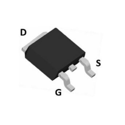
+8618001811078

QUICK CALL

Working hours:

Mon-Sat:9.30am to 7.00pm
Low Voltage Mosfet

Low Voltage Mosfet

1.00 - 10.00 USD ($)/Piece

Product Details:

X

Low Voltage Mosfet Price And Quantity

  • 10000 Piece
  • 1.00 - 10.00 USD ($)/Piece

Low Voltage Mosfet Trade Information

  • 20000 Piece Per Month
  • 7-15 Days
  • Asia Australia Central America North America South America Eastern Europe Western Europe Middle East Africa

Product Description

Description:

The RM series products utilizes Norsem's outstanding standard turbo process and packaging techniques to achieve ultral low on-resistance and low gate charge and to provide the industry's best-in-class performance. These features make this series products extremely efficient, temperature characteristics and reliable for use in power management, synchronous rectification, battery protection, load switch and a wide variety of other applications.

Features and Benefits:


  • Standard Turbo MOSFET process technology.
  • Optimized the cell structure.
  • Low on-resistance and low gate charge.
  • Featuring low switching and drive losses.
  • Fast switching and reverse body recovery.
  • High ruggedness and robustness.

Main Product Characteristics :

V(BR)DSS

30V

RDS(ON)

5.8mΩ(max.)

ID

100A

Absolute Maximum Ratings  (TC=25oC unless otherwise specified)

Parameter

Symbol

Max.

Unit

Drain-Source Voltage

VDS

30

V

Gate-to-Source Voltage

VGS

+ 20

V

Continuous Drain Current, @ Steady-State 1

ID @ TC = 25oC

100

A

Continuous Drain Current, @ Steady-State

ID @ TC = 100oC

68

A

Pulsed Drain Current 2

IDM

400

A

Power Dissipation

PD @TA = 25oC

83

W

PD @TA = 100oC

37.8

Linear Derating Factor

TA = 25oC

0.66

W/oC

Single Pulse Avalanche Energy3

EAS

780

mJ

Junction-to-Case

RθJC

0.6

oC/W

Junction-to-Ambient (PCB Mounted, Steady-State) 4

RθJA

62.5

oC/W

Operating Junction and Storage Temperature Range

TJ /TSTG

-55 to + 150

oC

Electrical Characteristics (TC=25oC unless otherwise specified)

Parameter

Symbol

Conditions

Min.

Typ.

Max.

Unit

Drain-to-Source Breakdown Voltage

V(BR)DSS

VGS=0V, ID=250μA

30

-

-

V

Drain-to-Source Leakage Current

IDSS

VDS=30V, VGS=0V

-

-

1

uA

TJ=125oC

-

-

50

Gate-to-Source Forward Leakage IGSS

IGSS

VGS =20V

-

-

100

nA

VGS =-20V

-

-

-100

Static Drain-to-Source On- Resistance

RDS (on)

VGS=10V, ID=50A

-

4.3

5.8

mΩ

VGS=4.5V, ID=15A

-

5.2

7.5

Gate Resistance

Rg

f-1MHz

-

1.8

-

Ω

Gate Threshold Voltage

VGS (th)

VDS=VGS, ID=250uA

1.0

1.6

2.6

V

Input Capacitance

Ciss

VGS=0V, VDS=5V
f=1MHz

-

2180

-

pF

Output Capacitance

Coss

-

270

-

Reverse transfer capacitance

Crss

-

210

-

Total Gate Charge

Qg

ID=30A, VDS=24V, VGS=10V

-

47.2

-

nC

Gate-to-Source Charge

Qgs

-

8.8

-

Gate-to-Drain("Miller") Charge

Qgd

-

9.6

-

Turn-on Delay Time

td (on)

VGS=4.5V, VDD=20V,

ID=60A, RGEN=1.8Ω

-

12.3

-

nS

Rise Time

tr

-

87.3

-

Turn-Off Delay Time

td (off)

-

140

-

Fall Time

tf

-

82.4

-

Source-Drain Ratings and Characteristics

Parameter

Symbol

Conditions

Min.

Typ.

Max

Unit

Continuous Source Current

(Body Diode)

Is

MOSFET symbol showing

the integral reverse

p-n junction diode.

-

-

100

A

Pulsed Source Current (Body Diode)

Ism

-

-

400

A

Diode Forward Voltage

VSD

IS=20A, VGS=0V

-

0.9

1.2

V

Reverse Recovery Time

trr

TJ = 25oC, IF =30A, di/dt =

100A/μs

-

16.5

-

ns

Reverse Recovery Charge

Qrr

-

6.5

-

uC

Notes :

1. Pulse test: Pulse Width≤300us, Duty cycle ≤2%.
2. Repetitive rating; pulse width limited by max. junction temperature.
3. L=0.5mH, VDD=15V, Rg=25Ω,TJ=25oC.
4. Device mounted on FR-4 PCB, 1inch x 0.85inch x 0.062 inch.

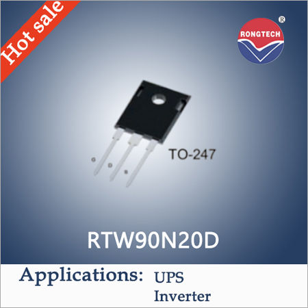
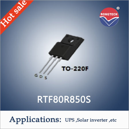
Other Products in 'Mosfet Power Semiconductor' category


We are accepting inquiries from these countries India, Sri Lanka, Pakistan, Bangladesh, Afghanistan and Nepal.
Back to top